
Sungkyunkwan UniversityNanoEnergy & NanoSensors Laboratory Lab
Research
Research Field
Research Field
Nanofabrications

Nanomaterials describe, in principle, materials of which a single unit is sized (in at least one dimension) between 1 to 1000 nanometres (10-9 meter) but usually is 1 to 100 nm. A nanostructure is a structure of intermediate size between microscopic and molecular structures. Materials with structure at the nanoscale often have unique optical, electronic, or mechanical properties. Our group studies large-area uniform and cost-effective nanostructures through anodic oxidation, deposition, layer-by-layer(LbL) self-assembly, and wet chemistry. In order to improve the surface characteristics, we utilize various surface treatment techniques such as plasma, UV, and nanoscale coating. In our group, we are trying to characterize morphological, mechanical, electrical, optical, and wetting properties of nanostructures and nanomaterials. Also, environmental stability of nanomaterials and nanostructures is one of key interesting properties for industrial applications.
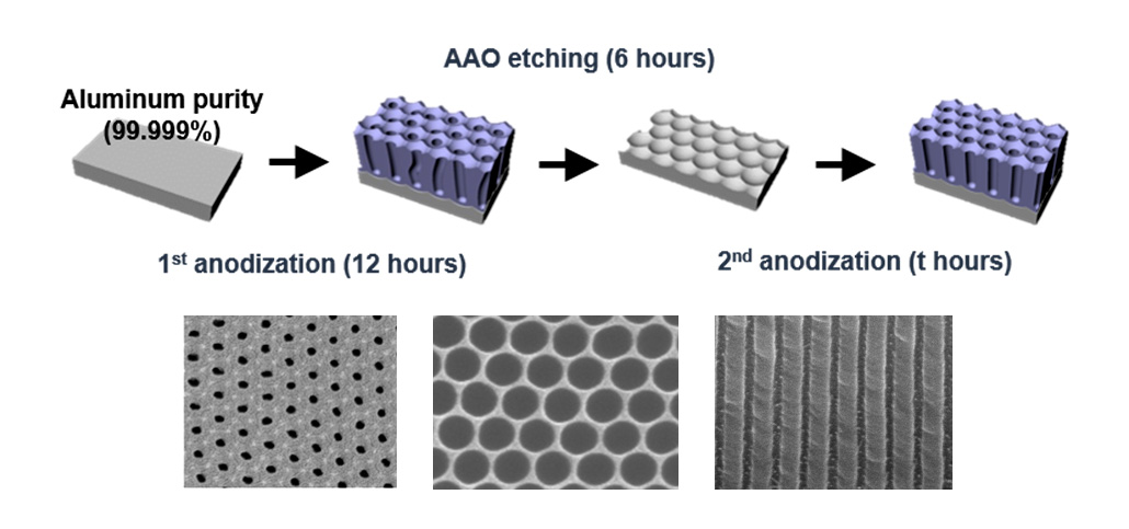
Anodization
Anodizing process simply creates large-area, uniform nanoporous structures on the surface of metals such as aluminum (Al) & titanium (Ti). We mainly fabricate nanoporous anodic aluminum oxide (AAO) which has high tunability in dimensions such as pore size, thickness, and shape by adjusting anodization and widening time. We also fabricate nanoporous titanium dioxides (TiO2) for various photocatalytic applications.
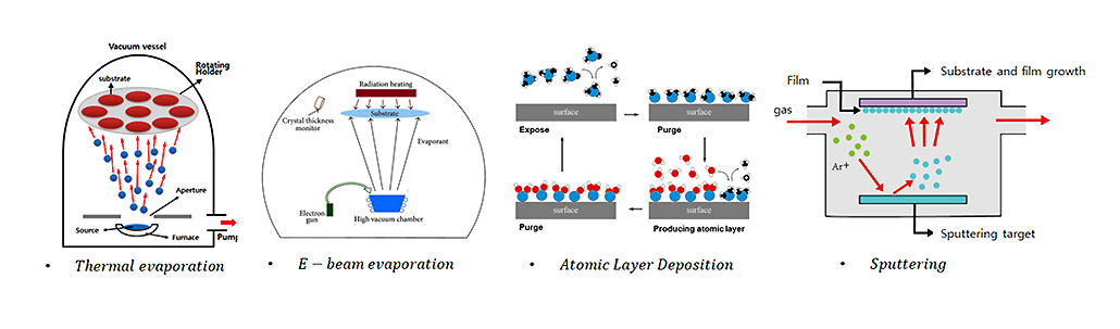
Deposition Methods
In our group, various deposition methods are used to control morphological, electrical, optical, and mechanical properties of material surfaces. Thermal evaporation proceeds under vacuum where target elemental materials can be deposited in form of a thin film by heating material placed on a boat. E-beam evaporation uses electron beam to heat a boat and evaporates target materials. Atomic layer deposition (ALD) is a deposition technique that utilizes a surface magnetic saturation to ensure surface uniformity that is critical to nano-device fabrication. Sputtering is a process whereby particles are ejected from a solid target material due to bombardment of the target by energetic particles, particularly gas ions in a laboratory.
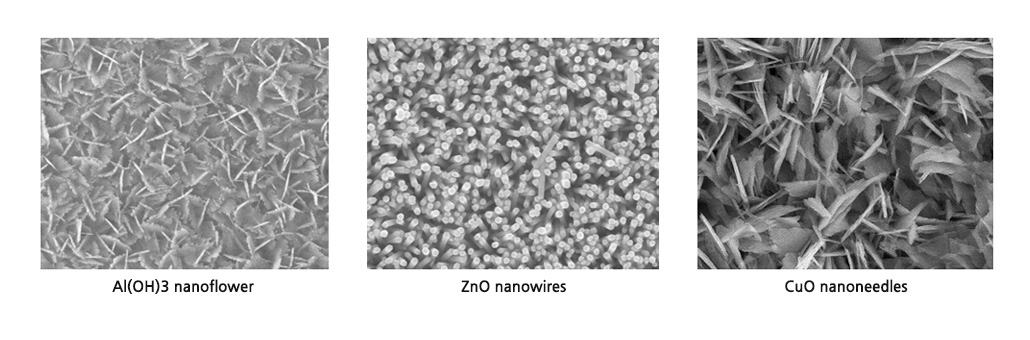
Wet chemical process
Our group uses wet chemical processes without vacuum to produce high-throughput, large-area and cost-effective nanostructures of various types of metal oxides and hydroxides. Al, Zn and Cu films can be used to produce nanostructured Al(OH)3, ZnO, and CuO.
Layer-by-layer self-assembly (LbL)
Layer-by-Layer self-assembly is a simple and easy dipping method to deposit target material on the substrate without any vacuum process. The good coverage is one of strength points of LbL deposition. The uniform deposition is possible on the nano/microstructured substrate. We utilize this technique to fabricate large-area, low-cost and flexible triboelectric nanogenerators with various organic/inorganic substrates such as PET, cotton and etc.
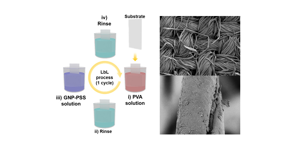 Schematic image of LbL process and FE-SEM image of LbL processed textile